- 您现在的位置:买卖IC网 > Sheet目录2000 > IDT5T9890NLI8 (IDT, Integrated Device Technology Inc)IC CLK DRIVER 2.5V PLL 68-VFQFPN
28
INDUSTRIALTEMPERATURERANGE
IDT5T9890
EEPROM PROGRAMMABLE 2.5V PROGRAMMABLE SKEW PLL CLOCK DRIVER
EEPROMOPERATION
(see I2C Interface Definition for the EEPROM instructions)
TheIDT5T9890canalsostoreitsconfigurationininternalEEPROM. Thecontentsofthedevice’sinternalprogrammingregisterscanbesavedtotheEEPROM
by issuing a save instruction (ProgSave) and can be loaded back to the internal programming registers by issuing a restore instruction (ProgRestore). To
initiate a save or restore, only two bytes are transferred. The Device Address is issued with the read/write bit set to ‘0’ followed by the appropriate Command
Code. The save or restore instruction executes after the STOP condition is received, during which time the IDT5T9890 will not generate Acknowledge bits.
The device is ready to accept a new programming instruction once it Acknowledges its 7-bit address. The time it takes for the save and restore instructions
to complete depends on the PLL oscillator frequency, FVCO. The restore time, TRESTORE, and the save time, TSAVE, can be calculated as follows:
TRESTORE = 1.23X10⁹/FVCO
(mS)
TSAVE = 3.09X10⁹/FVCO + 52
(mS)
In order for the save and restore instructions to function properly, the IDT5T9890 must not be in power-down mode (PDmust be HIGH), and the PLL must
be enabled (PLL_EN must be LOW and Bit 57 = 0).
Onpower-upoftheIDT5T9890,anautomaticrestoreisperformedtoloadtheEEPROMcontentsintotheinternalprogrammingregisters. Theauto-restore
will not function properly if the device is in power-down mode (PD must be HIGH). The device’s auto-restore feature will function regardless of the state of
the PLL_EN pin or Bit 57. The IDT5T9890 will be ready to accept a programming instruction once it acknowledges its 7-bit I2C address. The time it takes
for the device to complete the auto-restore is approximately 3ms.
PROGRAMMINGNOTES
OncetheIDT5T9890hasbeenprogrammedeitherwithaProgWriteorProgRestoreinstruction,thedevicewillattempttoachievephaselockusingthenew
PLLconfiguration. IfthereisavalidREFandFBinputclockconnectedtothedeviceanditdoesnotachievelock,theusershouldissueaProgReadinstruction
to confirm that the PLL configuration data is valid.
Onpower-upandbeforetheautomaticProgRestoreinstructionhascompleted,theinternalprogrammingregisterswillcontainthevalueof‘0’forallbits95:0.
ThePLLwillremainattheminimumfrequencyandwillnotachievephaselockuntilaftertheautomaticrestoreiscompleted. Iftheoutputsareenabledbythe
nSOE pins, the outputs will toggle at the minimum frequency. If the outputs are disabled by the nSOE pins and the OMODE pin is set HIGH, the nQ[1:0] and
QFB are stopped HIGH, while QFB is stopped LOW.
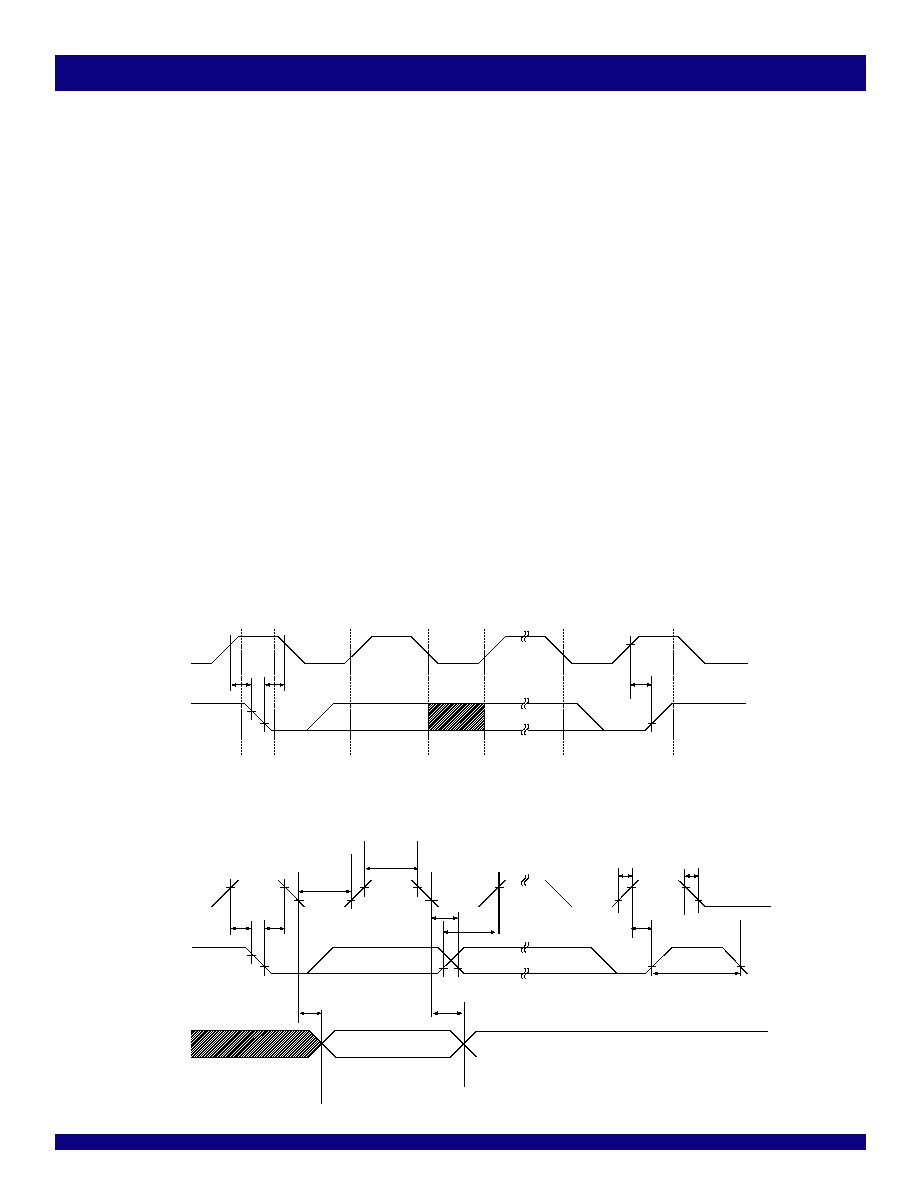
SCLK
SDA
tSU:START
tSU:STOP
STOP
Data can
change
Address or data
valid
tHD:START
START
SCLK
SDA IN
tSU:START
tSU:STOP
tHD:START
tLOW
tHIGH
tHD:DATA
tSU:DATA
tBUF
tR
tF
tOVD
SDA OUT
Figure 1: I2C Timing Data
发布紧急采购,3分钟左右您将得到回复。
相关PDF资料
IDT5V19EE604NDGI8
IC PLL CLK GEN 200MHZ 28VFQFPN
IDT5V40501DVG
IC CLK GEN PLL 160MHZ 8TSSOP
IDT5V41064NLGI
IC CLK GEN 1:1 16QFN
IDT5V41066PGG
IC CLK GEN SPRED SPECTRM 20TSSOP
IDT5V49EE901NLGI8
IC PLL CLK GEN 200MHZ 32VFQFN
IDT5V49EE902NLGI
IC CLOCK GEN PLL 500MHZ 32VFQFPN
IDT5V49EE904NLGI8
IC PLL CLK GEN 200MHZ 32VFQFN
IDT821024PPG
IC PCM CODEC QUAD NONPROG 44TQFP
相关代理商/技术参数
IDT5T9891NLGI
功能描述:IC CLK DRIVER 2.5V PLL 68-VFQFPN RoHS:是 类别:集成电路 (IC) >> 时钟/计时 - 时钟发生器,PLL,频率合成器 系列:- 标准包装:39 系列:- 类型:* PLL:带旁路 输入:时钟 输出:时钟 电路数:1 比率 - 输入:输出:1:10 差分 - 输入:输出:是/是 频率 - 最大:170MHz 除法器/乘法器:无/无 电源电压:2.375 V ~ 3.465 V 工作温度:0°C ~ 70°C 安装类型:* 封装/外壳:* 供应商设备封装:* 包装:*
IDT5T9891NLGI8
功能描述:IC CLK DRIVER 2.5V PLL 68-VFQFPN RoHS:是 类别:集成电路 (IC) >> 时钟/计时 - 时钟发生器,PLL,频率合成器 系列:- 标准包装:39 系列:- 类型:* PLL:带旁路 输入:时钟 输出:时钟 电路数:1 比率 - 输入:输出:1:10 差分 - 输入:输出:是/是 频率 - 最大:170MHz 除法器/乘法器:无/无 电源电压:2.375 V ~ 3.465 V 工作温度:0°C ~ 70°C 安装类型:* 封装/外壳:* 供应商设备封装:* 包装:*
IDT5T9891NLI
功能描述:IC CLK DRIVER 2.5V PLL 68-VFQFPN RoHS:否 类别:集成电路 (IC) >> 时钟/计时 - 时钟发生器,PLL,频率合成器 系列:- 标准包装:39 系列:- 类型:* PLL:带旁路 输入:时钟 输出:时钟 电路数:1 比率 - 输入:输出:1:10 差分 - 输入:输出:是/是 频率 - 最大:170MHz 除法器/乘法器:无/无 电源电压:2.375 V ~ 3.465 V 工作温度:0°C ~ 70°C 安装类型:* 封装/外壳:* 供应商设备封装:* 包装:*
IDT5T9891NLI8
功能描述:IC CLK DRIVER 2.5V PLL 68-VFQFPN RoHS:否 类别:集成电路 (IC) >> 时钟/计时 - 时钟发生器,PLL,频率合成器 系列:- 标准包装:39 系列:- 类型:* PLL:带旁路 输入:时钟 输出:时钟 电路数:1 比率 - 输入:输出:1:10 差分 - 输入:输出:是/是 频率 - 最大:170MHz 除法器/乘法器:无/无 电源电压:2.375 V ~ 3.465 V 工作温度:0°C ~ 70°C 安装类型:* 封装/外壳:* 供应商设备封装:* 包装:*
IDT5T989X-982X-M1
功能描述:KIT FOR 5T989X-982X RoHS:否 类别:编程器,开发系统 >> 评估演示板和套件 系列:- 标准包装:1 系列:- 主要目的:电信,线路接口单元(LIU) 嵌入式:- 已用 IC / 零件:IDT82V2081 主要属性:T1/J1/E1 LIU 次要属性:- 已供物品:板,电源,线缆,CD 其它名称:82EBV2081
IDT5T9950APFGI
功能描述:IC CLK BUFFER/DVR 1:10 32TQFP RoHS:是 类别:集成电路 (IC) >> 时钟/计时 - 时钟发生器,PLL,频率合成器 系列:TurboClock™ II JR 标准包装:1,000 系列:- 类型:时钟/频率合成器,扇出分配 PLL:- 输入:- 输出:- 电路数:- 比率 - 输入:输出:- 差分 - 输入:输出:- 频率 - 最大:- 除法器/乘法器:- 电源电压:- 工作温度:- 安装类型:表面贴装 封装/外壳:56-VFQFN 裸露焊盘 供应商设备封装:56-VFQFP-EP(8x8) 包装:带卷 (TR) 其它名称:844S012AKI-01LFT
IDT5T9950APFGI8
功能描述:IC CLK BUFFER/DVR 1:10 32TQFP RoHS:是 类别:集成电路 (IC) >> 时钟/计时 - 时钟发生器,PLL,频率合成器 系列:TurboClock™ II JR 标准包装:1,000 系列:- 类型:时钟/频率合成器,扇出分配 PLL:- 输入:- 输出:- 电路数:- 比率 - 输入:输出:- 差分 - 输入:输出:- 频率 - 最大:- 除法器/乘法器:- 电源电压:- 工作温度:- 安装类型:表面贴装 封装/外壳:56-VFQFN 裸露焊盘 供应商设备封装:56-VFQFP-EP(8x8) 包装:带卷 (TR) 其它名称:844S012AKI-01LFT
IDT5T9950PFGI
功能描述:IC CLK BUFFER/DVR 1:10 32TQFP RoHS:是 类别:集成电路 (IC) >> 时钟/计时 - 时钟发生器,PLL,频率合成器 系列:TurboClock™ II JR 标准包装:2,000 系列:- 类型:PLL 频率合成器 PLL:是 输入:晶体 输出:时钟 电路数:1 比率 - 输入:输出:1:1 差分 - 输入:输出:无/无 频率 - 最大:1GHz 除法器/乘法器:是/无 电源电压:4.5 V ~ 5.5 V 工作温度:-20°C ~ 85°C 安装类型:表面贴装 封装/外壳:16-LSSOP(0.175",4.40mm 宽) 供应商设备封装:16-SSOP 包装:带卷 (TR) 其它名称:NJW1504V-TE1-NDNJW1504V-TE1TR